February 3, 2026
MOSFET Process Characterization Guide
Extracting simple MOSFET model variables from a complex model file.
Reference code for this blog is available here.
Introduction
Often times when working with MOSFETs you may want to work a problem out by hand. You may do this for any number of reasons, but one may be just to do some quick calculations by hand as opposed to setting up a full simulation. This way, you can do the math symbolically and compute any parameters you may be looking for.
However, we may only have the simulation model, and the equations for using these models get increadibly complicated very quickly.
Thankfully, we can use "process characterization" which allows us to model the MOSFET using two relatively simple equations (NMOS shown, PMOS similar):
The first equation is the MOSFET drain current equation, and the second equation is the body-effect equation. Using these equations we can determine just a few parameters that model the MOSFET fairly well: , , , , and . Note that these equations are for NMOS devices, PMOS devices are similar, see my note in the conclusion for more info.
For this demo, I'll be using LTSpice and this advanced MOSFET model. As you can see from the model file, it is much more complicated than the above equations and parameters.
Finding and
To get started, we will first be finding the and values.
To get started, we're going to bias up our MOSFET by sending a bias current, through it. We have the MOSFET in a diode-connected orientation, this means the gate and drain are tied together and at the same potential. We also have a current source which will be used to invoke the body-effect by causing the source and body to be at different potentials.
Here is the LTSpice schematic:
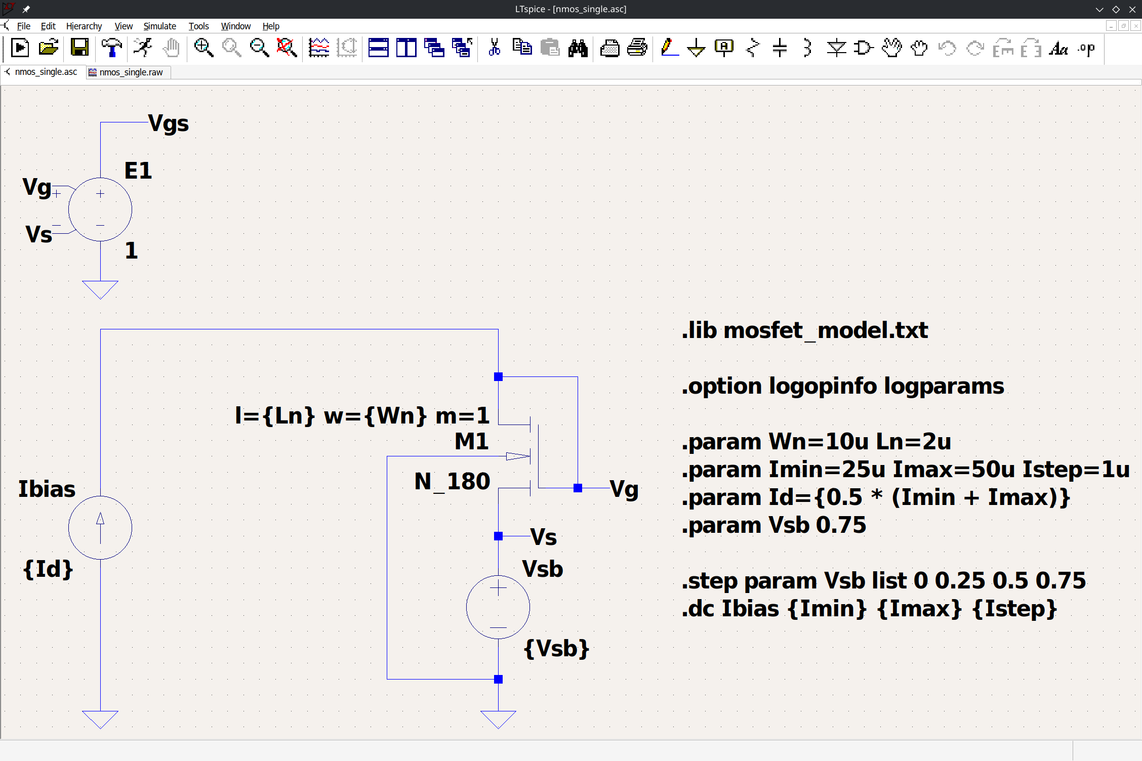
For now, we are only interested in the dc sweep of where .
Note that our value is relatively large for this process, this is ideal to minimize the effects of . This is also a good time to mention that all of these values may vary depending on the process you are trying to characterize, you should use appropriate bias points, and MOSFET geometries for your process.
Since we're minimizing the channel length modulation, , we will remove it from the drain current equation. Additionally, since we're using the step where , we can say that and thus we get the simplified drain current equation:
We can then rearrange this equation as such:
If you look closely at the final line, you can see it is in the form of where both and contain the parameters we wish to extract from the model, and and are values we can plot in LTSpice.
Finally we can extract and :
In order to analyze our LTSpice data, we will first run the simulation, then we will plot the V(Vgs) node, then finally we will need to export it as a text file, here I've saved it as nmos_single_data.txt:
Next, we need to perform a linear fit on the data, to do so, we're going to use python as it's pretty easy to work with. We use the numpy polyfit method to fit the data. below is a quick snippet showing a simple example of how to do this:
# MOSFET length and width.
L = 2e-6
W = 10e-6

# Make sure we're fitting over the sqrt of the drain current.
sqrt_i_d = np.sqrt(i_d)

# Perform the linear fit.
m, b = np.polyfit(sqrt_i_d, v_gs, deg=1)

# Extract the process variables.
k_prime = (2 * L) / (W * (m**2))
v_t0 = b # This is only Vt0 if the source-body voltage is 0V!
Finding
Let's recall the threshold voltage equation from above:
First, in order to estimate , we need to eliminate from the equation. To do this, we'll define (where refers to a different step) such that:
As before when we found , we can do the same thing, except we will use different values, where . From the same LTSpice schematic above, you can see that I used values of , , and , (along with our step, where ).
After we calculate these values, we can eliminate by creating two ratios:
As you can see, the value will cancel out in each ratio, leaving us with only the unknown value. In order to extract the value, we will sweep through a range of values in order to find the value which most accurately represents the "observed" ratio value. So to be more precise, we will minimize the 2-norm error, , defined by the following:
Let's see what this looks like in python:
# Calculate our alpha values.
a1 = v_t_vals[1] - v_t_vals[0]
a2 = v_t_vals[2] - v_t_vals[0]
a3 = v_t_vals[3] - v_t_vals[0]

# Lambda function which returns the portion of the
# body-effect equation which is multiplied by gamma.
# sqrt( 2phi_f + Vsb ) - sqrt( 2phi_f )
gamma_term = lambda tpf, vb: np.sqrt(tpf + vb) - np.sqrt(tpf)

# Lambda functions which calculate the e1 and e2 errors for a given 2phi_f value.
e1 = lambda tpf: (
    gamma_term(tpf, v_b_vals[2]) / gamma_term(tpf, v_b_vals[1])
) - (a2 / a1)
e2 = lambda tpf: (
    gamma_term(tpf, v_b_vals[3]) / gamma_term(tpf, v_b_vals[2])
) - (a3 / a2)

# Lambda function to calculate the two-norm error.
twonorm = lambda e1, e2: np.sqrt(e1**2 + e2**2)

# Create a sweep of 2phi_f values within a reasonable range.
tpf_vals = np.linspace(0.3, 1.3, 10_000)
# Calculate the two-norm residual value for each 2phi_f estimate.
residuals = np.array([twonorm(e1(tpf), e2(tpf)) for tpf in tpf_vals])

# Get the index of the lowest two-norm error.
best_index = np.argmin(residuals)
# Extract 2phi_f to be the best estimate
two_phi_f = tpf_vals[best_index]
Finding
Now that we have a value for , we can take another look at the threshold voltage equation:
Once again, we see it's in the form of a linear function, where is the value, is the value. From this, we can extract which is the slope, , of this linear fit.
Just like before, we can use numpy to extract this value:
# Setup the x and y values for the linear fit.
# Note: we're using some variables and lambda functions from the 2phi_f step.
x_vals = np.array([gamma_term(two_phi_f, vb) for vb in v_b_vals])
y_vals = v_t_vals - v_t_vals[0]

# We only need the m value since we moved the intercept over. y-b = mx
m = np.polyfit(x_vals, y_vals, deg=1)
# Extract our estimated gamma value.
gamma = m
Finding
Finally, all we have left to estimate is the value. This value represents the channel length modulation, and as such is dependent on the device geometry. Because of this, we must calculate the for each channel length we may be interested in, so we'll calculate a few values.
Let's recall the full drain current equation:
As you can see, affects the drain current proportional to the drain-source voltage. This means we can simplify the drain current equation as such:
Where is the drain current without the term. Once again, we see this is in the form of a line, where the is , is , is , and is .
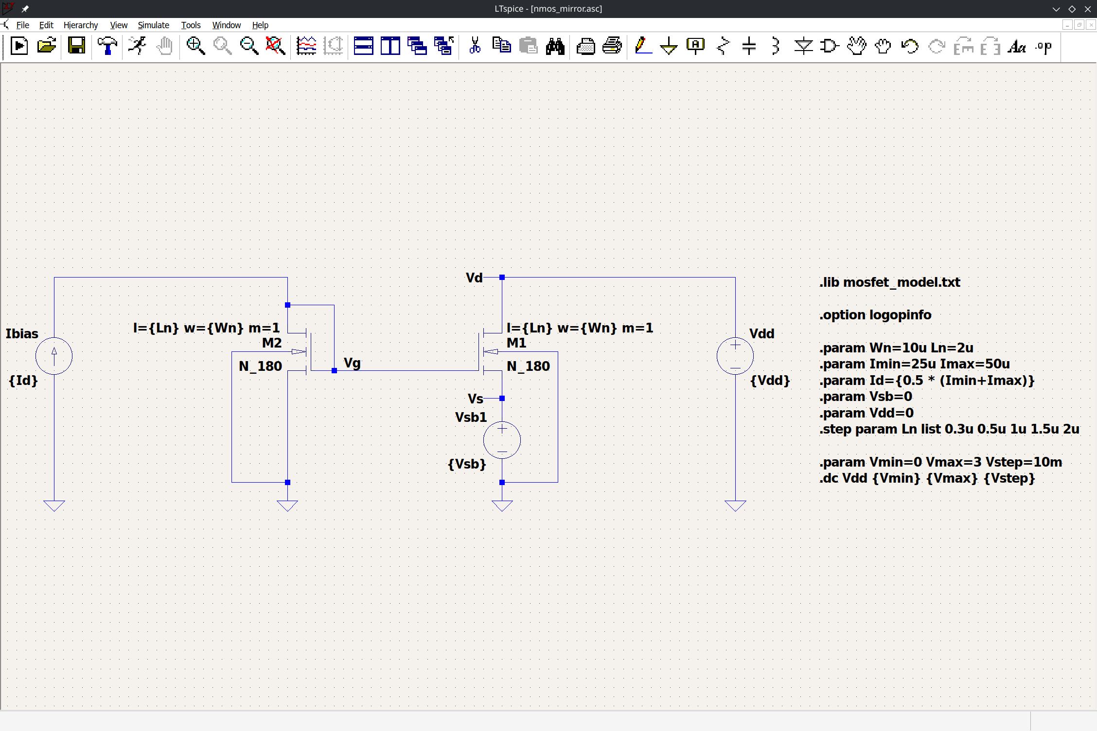
To set this up in LTSpice, we will use a simple current mirror, this let's us have two identical and matched MOSFETs which helps to cancel out any other process variations. We pass a bias current though the diode connected MOSFET which will bias up the second MOSFET, eliminating the other process characteristics. We can then vary the of the second MOSFET to see how affects it. Below is an image of the LTSpice schematic:
Let's briefly take a glance at what the plot looks like first to see what we're getting into:
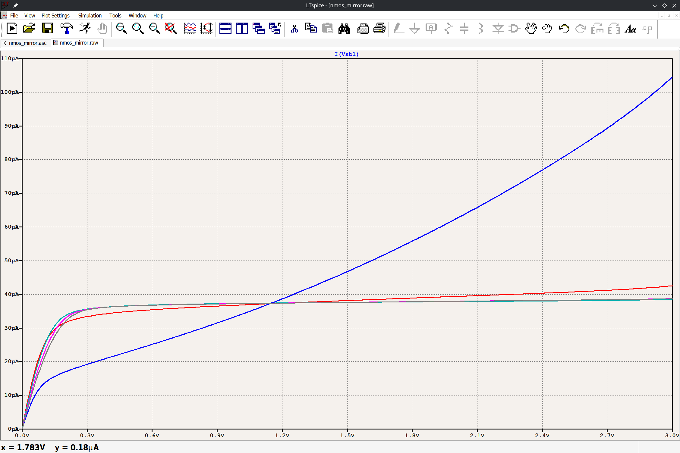
As you can see on the far left, the MOSFET is in the triode / linear region, this is not what we're looking for and there are different equations that model the MOSFET during this region. Secondly, on the far right you can see how the slope on some graphs continue to rise the higher gets, this is a phenomenon known as punch-through and again is a non-ideality we don't want to capture in our estimation.
In order to mitigate this and extract the best estimate we can, we want to take a relatively small slice of the plot, say , shortly after the MOSFET is saturated.
Once again, we can use python and numpy to do just that:
# Start linear fit at 700mV.
v_start = 0.7
# Use a 200mV slice.
v_range = 0.2
# Get the end of the slice.
v_end = v_start + v_range

# Array to store the lambda estimate for each channel length.
lambda_vals = []

# Iterate over each plot from LTSpice, one for each channel length.
for sweep in sweeps:
    # Create a mask to filter only the slice we're interested in.
    mask = (sweep.v_ds >= v_start) & (sweep.v_ds <= v_end)

    m, b = np.polyfit(sweep.v_ds[mask], sweep.i_d[mask], deg=1)

    # Since m = Id0 * lambda, and b = Id0
    # We can isolate lambda by doing m / b
    lambda_vals.append(m / b)
Conclusion
Finally! We have now fully process characterized the MOSFET model, and can use it however we please.
A quick note on PMOS devices:
All the voltages measured on a PMOS device must be inverted from the standard NMOS definition. For instance, on an NMOS should be on a PMOS device. If you take care to properly do all of the inversions, the same code which will characterize an NMOS will also characterize a PMOS. All values should be positive, except for .
For reference, here are the values I extracted from the demo model:
NMOS
| Parameter | Value |
|---|---|
PMOS
| Parameter | Value |
|---|---|
Finished here? See the latest posts or head home.
Questions, comments, or concerns? Contact me.